Welcome: Shenzhen leap electronic co.,ltd
Language:
 ∷
∷

∷
∷

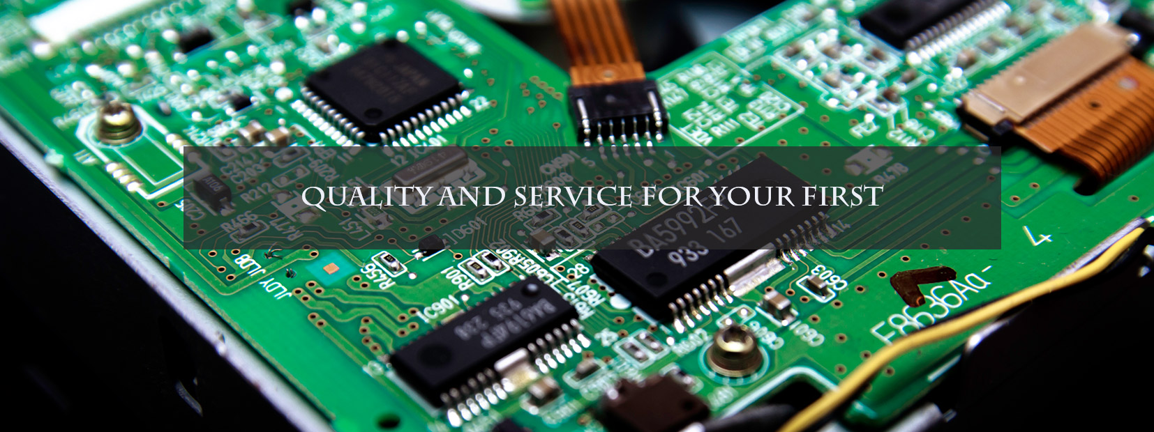
In today's industrially developed, PCB circuit boards are widely used in various electronic products. Depending on the industry, the color, shape, size, level, and materials of PCB boards are different. Therefore, it is necessary to have clear information on the design of the PCB board, otherwise it is prone to misunderstanding.
First, the definition of processing level is not clear
The single-panel design of the circuit board is in the TOP layer. If you do not explain the front and back, you may make the board to install the device without soldering.
Second, the large area of copper foil is too close to the outer frame
A large area of copper foil should be at least 0.2mm or more from the outer frame, because it is easy to cause the copper foil to rise and cause the solder resist to fall off when milling the shape to the copper foil.
Third, draw pads with padding
Draw a pad with a pad to pass the DRC check when designing the line, but it is not suitable for processing. Therefore, the pad cannot directly generate solder resist data. When the solder resist is applied, the pad area will be covered by the solder resist, resulting in the device. Welding is difficult.
Fourth, the electric ground layer is the flower pad and the connection
Because the circuit board is designed as a flower pad mode power supply, the ground layer is opposite to the actual printed circuit board image. All the wires are isolated wires. Care should be taken when drawing several sets of power supplies or several ground isolation wires, so that no gaps can be left. The two groups of power supplies are short-circuited and cannot cause the connection area to be blocked.
Five, the characters are placed
The character cover pad SMD soldering piece brings inconvenience to the printed board on-off test and component soldering. Character design is too small, making screen printing difficult, too large will make characters overlap each other, difficult to distinguish.
Six, surface mount device pads are too short
For the continuity test, for a too dense surface mount device, the spacing between the two legs is quite small, and the pads are also relatively thin. The test pins must be placed up and down, such as the pad design is too short, although not Affects device mounting, but causes the test pin to be misplaced.
Seven, single-sided pad aperture setting
The single-sided pad of the circuit board is generally not drilled. If the hole is to be marked, its aperture should be designed to be zero. If a numerical value is designed, when the drilling data is generated, the hole coordinates appear at this position, and a problem occurs. Single-sided pads such as drilled holes should be specially marked.
Eight, the overlap of the pads
In the drilling process, the drill bit is broken due to multiple drilling at one location, resulting in damage to the hole. The two holes in the multi-layer board overlap, and the negative film is formed as a spacer disk, which causes scrapping.
Nine, too many filling blocks in the design or filled blocks filled with very thin lines
There is a loss of the generated light data, and the light data is not complete. Because the filling block is drawn by lines one by one during the processing of the light drawing data, the amount of light drawing data is quite large, which increases the difficulty of data processing.
Ten, graphics layer abuse
Some useless connections were made on some graphics layers. The original four-layer board was designed with more than five layers, which caused misunderstanding. Violation of routine design. The graphics layer should be kept complete and clear during design.
Contact: Lillian Zhu
Phone: 008613928048496
Tel: 0755-28628518
Email: leappcb@163.com,sales@leappcb.com
Add: Hongtian industry,baoan area,shenzhen city,guangdong ,china
 Lillian
 leappcb