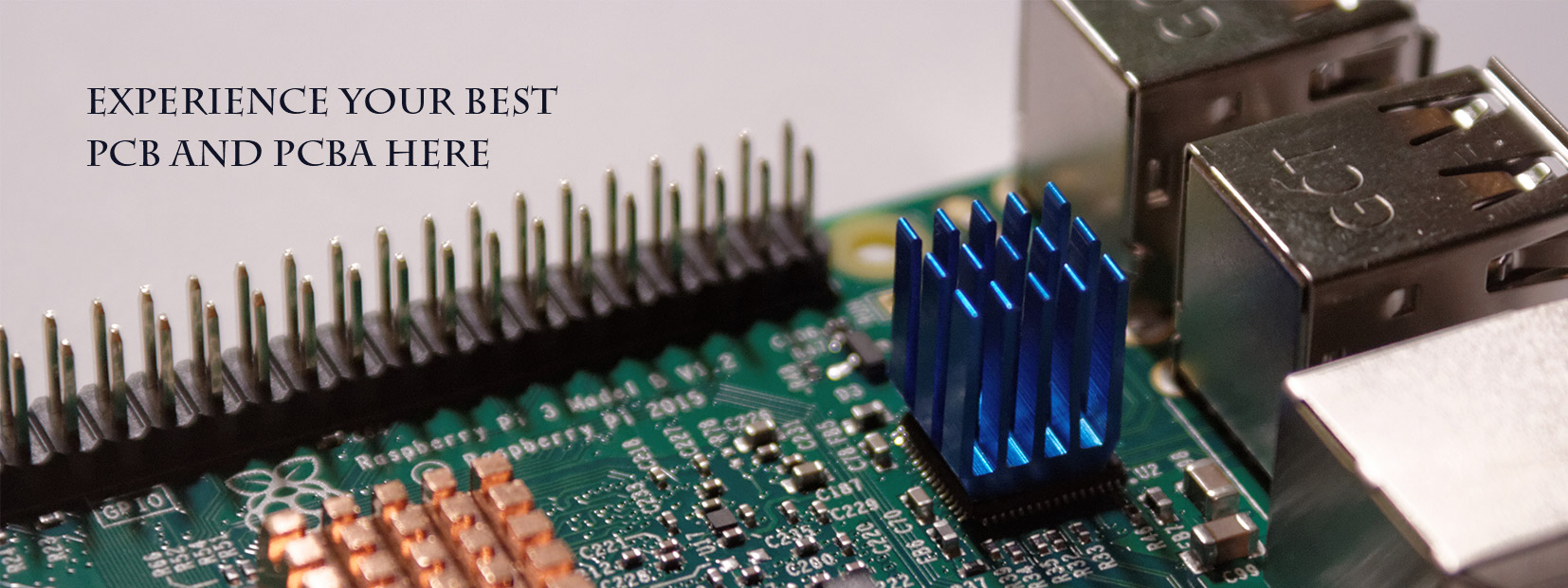
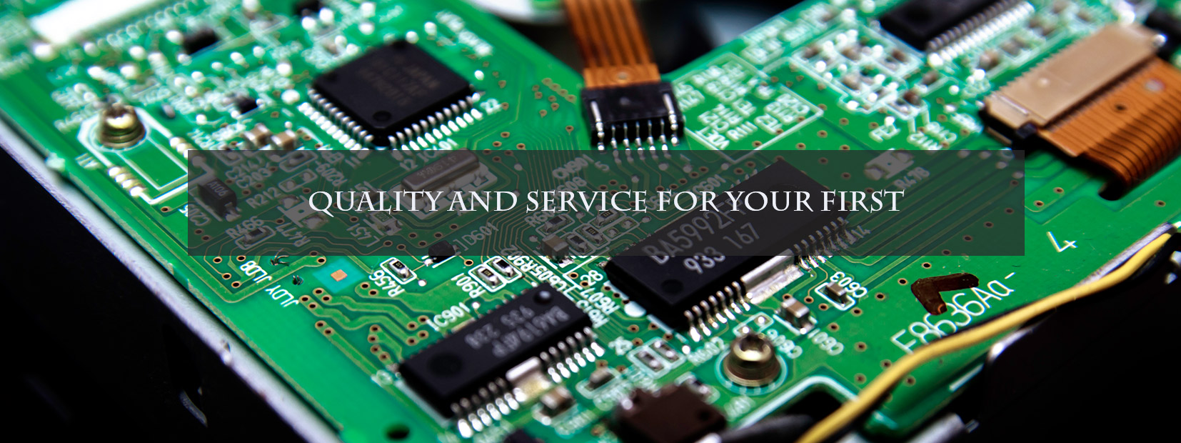
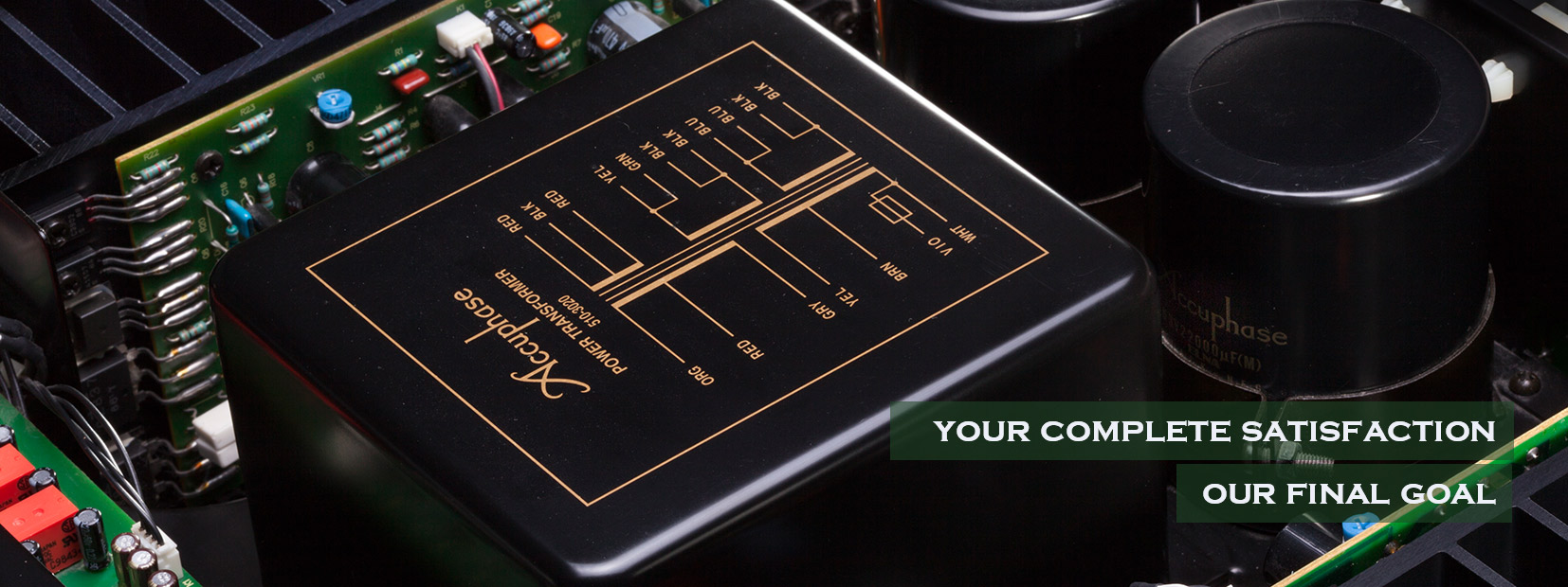
Welcome: Shenzhen leap electronic co.,ltd
Language:
 ∷
∷

∷
∷
1. Storage environment and transportation: This is the middle link between the circuit board factory and the patch factory. Generally, the circuit board rarely appears in stock, but the general inventory requires the storage environment to have suitable dry humidity, complete packaging, and lightest in the transportation process. Take it lightly, do not allow the vacuum packaging to be damaged for a long time to store. The theoretical placement time of the tin plate is one month, but the best time for soldering is 48 hours. If the storage time is more than one month, it is recommended to return to the circuit board factory for special use. The potion is cleaned and baked.
2. The operation at the time of shipment is not in accordance with the operation specification: the line industry is a workshop environment, and the staff's standard operation requirements are extremely strict. Especially in the circuit board production process, all the chemical reaction environment is required, so the infiltration of impurities is not allowed. After the tin-spraying process of the board is completed, the subsequent series requires employees to wear anti-static gloves. Because the finger sweat or stain directly contacts the surface, the surface will be oxidized. If the defect is extremely difficult to find, it is irregularly presented. And the tin experiment is difficult to show.
3. Welding defects caused by warpage: The circuit board and components are warped during the welding process, and defects such as virtual welding and short circuit are generated due to stress deformation. Warpage is often caused by temperature imbalances in the upper and lower parts of the board. Warpage can also occur on large PCBs due to the weight of the board itself. The ordinary PBGA device is about 0.5mm away from the printed circuit board. If the device on the circuit board is large, the normal shape will be restored as the circuit board cools down, and the solder joint will be under stress for a long time. If the device is raised by 0.1mm, it will be enough. For the special product, the virtual soldering circuit can be used to reduce the warpage of the circuit board factory, or to make the appropriate size of the imposition. It should not be too large or too small.
4. The source of tin used for incoming materials: For material procurement, some circuit board factories are pursuing compression costs. When using tin-sprayed tin, the tin is recovered from the procurement industry, or the source of unstable content is generally low. There is a possibility of such a risk in the board factory, and it is recommended that you carefully select the supplier.
5. The tin furnace for tinning is not cleaned on time: the timely maintenance of the tin furnace is very important, because the tin is a vertical circulation process, the board surface will be under strong pressure, and the characters are not dry for those solder joints. The board will produce impact and fall off, deposit in the furnace, and evaporate at high temperature. If it is not cleaned for too much time, the surface will adhere.
Contact: Lillian Zhu
Phone: 008613928048496
Tel: 0755-28628518
Email: leappcb@163.com,sales@leappcb.com
Add: Hongtian industry,baoan area,shenzhen city,guangdong ,china
 Lillian
 leappcb