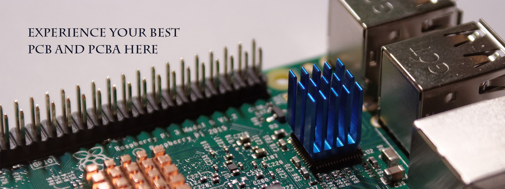
Welcome: Shenzhen leap electronic co.,ltd
Language:
 ∷
∷

∷
∷
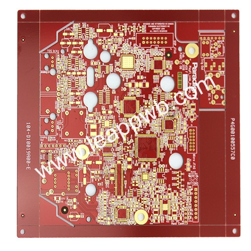
Production pattern: PCB
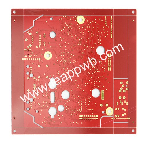
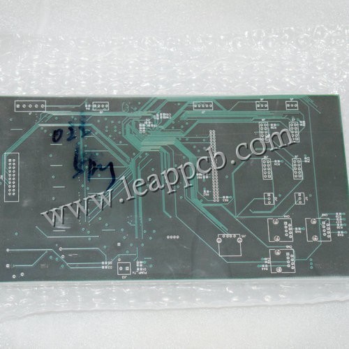
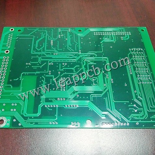
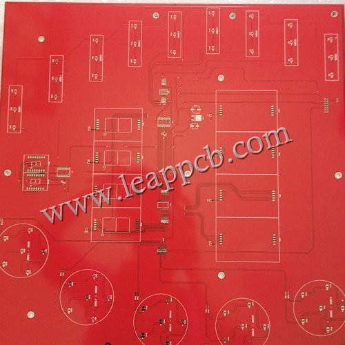
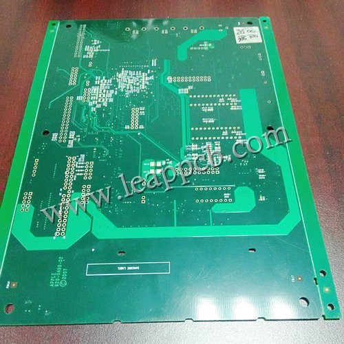
PCB layers: 8 layer circuit board
Plate: FR4
Type: custom
Packing: vacuum/air bubble bags/pearl cotton
Origin: China
HS Code: 8534009000
with the development of high density and high precision electronic products,the same requirements also have been provided for the pcb board.The most efficiency way to increase the pcb density is to deduce the number of via holes and design the buried blind holes precise.So the HDI PCB emerge at the right moment.
HDI board are compact products that designed for small capacity users.It's modular product with parallel design.One module capacity is 1000VA(1U in height),can be directly put into a 19" rack after natural cooling and 6 modules can be connected in parallel.This product adopts all digital signal process control(DSP) technology and multiple patent technology,have the capability of adapting load capacity in large scale and stronger short-term overload without load power and peak factors.
HDI pcb board is mainly made by using micro buried and blind hole technology,which can make the density of electronic circuit in the pcb board more higher.The HDI board drill can't done by normal process for the circuit density increased.
HDI board must take a non-mechanical drilling process, the "laser hole" is mainly used for the HDI hign density technology amongst many ways.
Generally,the HDI board is produced by build-up method,and the higher number of layers,the higher the technical level of the pcb board.
Also can reduce the cost of pcb.
If we produce the pcb as HDI board when the board density over 8 layer,the production cost will be cheaper than the traditional complicated lamilation process.
buried and blind via hole pcb,also known as HDI board,is often used in high-end product,such as mobile phone,GPS navigation and so on.
It is a manufacturing process that includes inner and outer circuits,drilling and hole metallization,which enable linking betwwn the interiors of the layers.
HDI board mostly used in phones,digital cameras,MP3,MP4,laptops,car electronics and other digital produces,especailly the mobile phone applications are widely used.
Contact: Lillian Zhu
Phone: 008613928048496
Tel: 0755-28628518
Email: leappcb@163.com,sales@leappcb.com
Add: Hongtian industry,baoan area,shenzhen city,guangdong ,china
 Lillian
 leappcb